| Digital
Pot 5206
reference:
PDF
file : AD5206
http://stage.itp.tsoa.nyu.edu/~kdm232/analog.html
http://stage.itp.nyu.edu/~ac1065/sculptwdataelect.htm
http://www.itp.nyu.edu/~caj240/analog/journal/1104.htm
http://stage.itp.tsoa.nyu.edu/~kdm232/analog.html
Greg's
shakar's digital Pot Example
http://stage.itp.nyu.edu/%7Egs41/pcomp/digitalpot.html
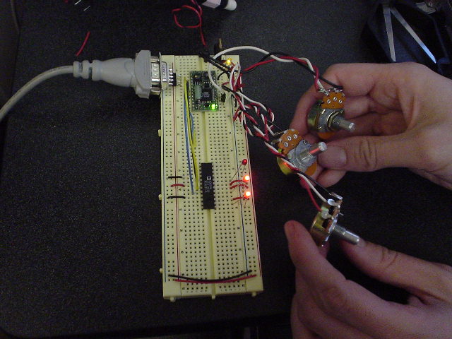
photo
from http://www.itp.nyu.edu/~caj240/analog/journal/1104.htm
Digital
Pot 5206 and PIC code
'****************************************************************
'* Name : UNTITLED.BAS *
'* Author : [select VIEW...EDITOR OPTIONS] *
'* Notice : Copyright (c) 2003 [select VIEW...EDITOR OPTIONS] *
'* : All Rights Reserved *
'* Date : 11/24/2003 *
'* Version : 1.0 *
'* Notes : *
'* : *
'****************************************************************
' This example uses the Analog Devices AD5206 chip which has 6 digitally
controlled pots.
' It assumes that you have:
' PIC D2(BX24 pin 7)* wired to the SDI pin (pin 7) of the AD5206 (data
input)
' PIC D3(BX24 pin 8)wired to the CLK pin (pin 8) of the AD5206 (clock
input)
' PIC B3(BX24 pin 6) wired to the CS pin (pin 5) of the AD5206 (Chip
Select Input)
' Vss pin
(pin 9) of the AD5206 is connecxted to ground
' GND pin (pin 4) of the AD5206 is connecxted to ground
' Vdd pin (pin 6) of the AD5206 is connecxted to +5 Volts
' There
are pots connected to PIC Porta.o,
' AD5206 pins 15,18,19 are connected to +5 volts
' AD5206 pins 14,17,20 are connected to the annodes (the longer legs)
of leds whose other legs are connected to ground
' Turning
the pots will adjust the brightnesses of the LEDs
Include "modedefs.bas"
Define OSC 20
TRISA =%11111111
potVar1
var Word
potVar2 var Word
potVar3 var Word
potVar11 var byte
potVar22 var byte
potVar33 var byte
address VAR byte
clkPin
var PORTD.3 'clkPin VAR byte
CSpin VAR PORTD.2 'CSpin var byte
dataVar VAR PORTB.3 'dataVar VAR byte
counter var byte
currentBit VAr byte
Main :
Pause 200
address
= 0
ADCON1 = %10000010 ' PORTA is analog
adcin 0, potVar1
adcin 1, potVar2
adcin 2, potVar3
Low PortB.3
'putpin(6,0)
potVar11 = potVar1 / 4
potVar22 = potVar2 / 4
potVar33 = potVar3 / 4
''----------------------------------------
'' potSDIout(dataPin,ClockPin,CSpin,address (potentiometer number),
'' data (0 - 255 minimum resistance to maximum resistance))
'potSDIout(7,8,6,0,potVar1)
'potSDIout(7,8,6,1,potVar2)
'potSDIout(7,8,6,2,potVar3)
''----------------------------------------------------
'' potSDIout(dataPin,ClockPin,CSpin,address
(potentiometer number),
'' data (0 - 255 minimum resistance to maximum resistance))
'potSDIout(portD.2,PORTD.3,PORTB.3,0,potVar1)
'potSDIout(portD.2,PORTD.3,PORTB.3,1,potVar2)
'potSDIout(portD.2,PORTD.3,PORTB.3,2,potVar3)
potSDIout(dataPin,
clkPin, CSpin, 0, potVar1)
potSDIout(dataPin, clkPin, CSpin, 1, potVar2)
potSDIout(dataPin, clkPin, CSpin, 2, potVar3)
Goto main
potSDIout(dataPin, clkPin, CSpin, address, datavar) :
'clkPin var PORTD.3 'clkPin VAR byte
'CSpin VAR PORTD.2 'CSpin var byte
'dataVar VAR PORTB.3'dataVar VAR byte
'counter var byte
'currentBit VAr byte
Low cSpin
Low clkpin
for counter
= 0 to 2
currentBit = getBit(address,(2 - counter))
dataPin,currentBit
High clkpin
Low clkpin
next
for counter
= 0 to 7
currentBit = getBit(dataVAR,(7 - counter))
dataPin,currentBit
High clkpin
Low clkpin
next
High CSpin
REturn
this
is the PIC and digital pot 5206 code from http://stage.itp.tsoa.nyu.edu/~kdm232/digipotz.htm
'************************************************************************
'* Name : digipotz.BAS
'* Author : Kari Martin
'* Notice : Copyright (c) 2002
'* Date : 11/9/02
'* Version : 1.0
'* Notes : pins A0 to A5 are temp sensors
'* : c3 SDI, c4 CLK, c5 CS pin
'
' C3 wired to the SDI pin (pin 7) of AD5206 (data input)
' C4 wired to the CLK pin (pin 8) of AD5206 (clock input)
' C5 wired to the CS pin (pin 5) of AD5206(Chip Select Input) ?
' AD5206 pins 15,18,19 are connected to +5 volts
' AD5206 pins 14,17,20 are connected to the annodes of leds
'************************************************************************
DEFINE
osc 4
INCLUDE "modedefs.bas"
' Set Debug
pin port
DEFINE DEBUG_REG PORTC
DEFINE DEBUG_BIT 7
DEFINE DEBUG_BAUD 9600
DEFINE DEBUG_MODE 1
' Define
ADCIN parameters
DEFINE ADC_BITS 10 ' Set number of bits in result
DEFINE ADC_CLOCK 3 ' Set clock source (3=rc)
DEFINE ADC_SAMPLEUS 50 ' Set sampling time in uS
output
portc.3
output portc.4
output portc.5
output portb.0
output portb.7
' Set PORTA
to all input
TRISA = %11111111
ADCON1 = %10000010
address
var byte
counter var byte
currentBit var byte
lf con
10 ' line feed charactger in ASCII
cr con 13 ' carriage return character in ASCII
Pause 500
address = 1
high portb.7
�attatch an LED, for a reset alert
pause 20
low portb.7
main:
high portb.0 'low CS
for counter=
0 to 255
low portb.0 'cs low
'low portc.4 'clk pin
'first
send out 3 address bits to choose a pot on the 5206
shiftout portc.3, portc.4, 1, [address/3]
'then
send out the 8 bits of data
shiftout portc.3, portc.4, 1,[counter]
counter=
counter + 1
high portb.0
'cs high
Pause 10 ' Wait.01 second
next
GoTo main
' Do it forever
-----------------------------------------------------------------
Digital
Pot 5026 and BXcode
' This example uses the Analog Devices AD5206 chip which
has 6 digitally controlled pots.
' It assumes that you have:
' BX24 pin 7 wired to the SDI pin (pin 7) of the AD5206 (data input)
' BX24 pin 8 wired to the CLK pin (pin 8) of the AD5206 (clock input)
' BX24 pin 6 wired to the CS pin (pin 5) of the AD5206 (Chip Select
Input)
' Vss pin (pin 9) of the AD5206 is connecxted to ground
' GND pin (pin 4) of the AD5206 is connecxted to ground
' Vdd pin (pin 6) of the AD5206 is connecxted to +5 Volts
' There are pots connected to BX24 pins 14,15,16
' AD5206 pins 15,18,19 are connected to +5 volts
' AD5206 pins 14,17,20 are connected to the annodes (the longer legs)
of leds whose other legs are connected to ground
' Turning the pots will adjust the brightnesses of the
LEDs
Option Explicit
dim potVar1 as byte
dim potVar2 as byte
dim potVar3 as byte
dim address as byte
Public Sub Main()
call delay(1.5)
address = 0
do
call putpin(6,0)
potVar1 = cbyte( ( getADC(16) \ 4 ) )
potVar2 = cbyte( ( getADC(15) \ 4 ) )
potVar3 = cbyte( ( getADC(14) \ 4 ) )
' potSDIout(dataPin,ClockPin,CSpin,address (potentiometer number), data
(0 - 255 minimum resistance to maximum resistance))
call potSDIout(7,8,6,0,potVar1)
call potSDIout(7,8,6,1,potVar2)
call potSDIout(7,8,6,2,potVar3)
loop
End Sub
Sub potSDIout(byVal dataPin as byte, byVal clkPin as byte, byVal CSpin
as byte, byVal address as byte, byVal data as byte)
dim counter as byte
dim currentBit as byte
call putpin(CSpin,0)
call putpin(clkpin,0)
for counter = 0 to 2
currentBit = getBit(address,(2 - counter))
call putPin(dataPin,currentBit)
call putpin(clkpin,1)
call putpin(clkpin,0)
next
for counter = 0 to 7
currentBit = getBit(data,(7 - counter))
call putPin(dataPin,currentBit)
call putpin(clkpin,1)
call putpin(clkpin,0)
next
call putpin(CSpin,1)
end Sub
|